


English
English

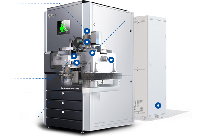
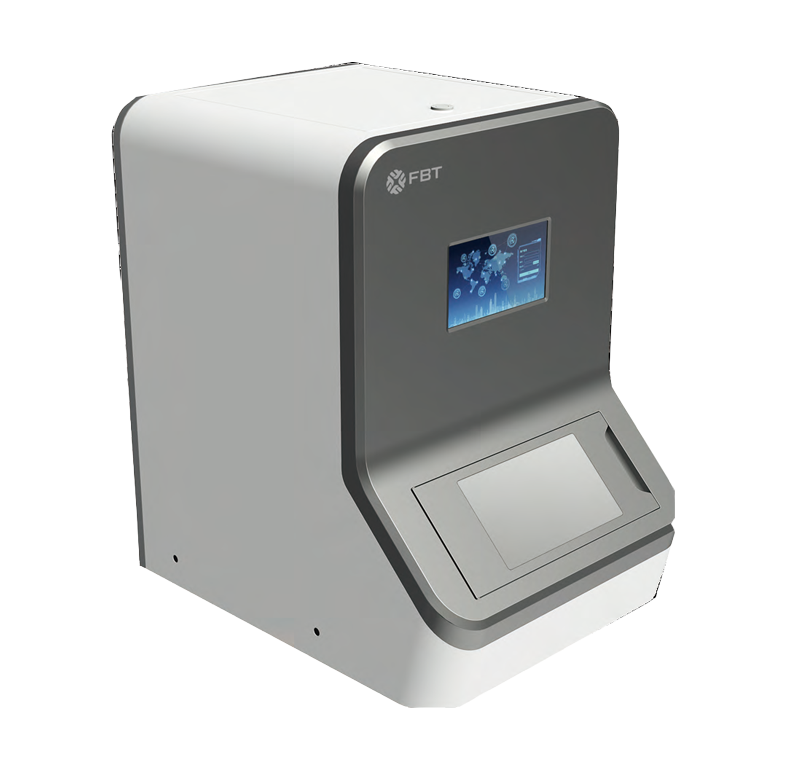
Owning our own intellectual property and propriety imaging technology, motion and circuit control. Focus e-Beam Technology produces its world's highest throughput scanning electron microscope (SEM), NavigatorSEM-100-SEMI(field emission). Enable imaging speed more than 10 times throughput of a conventional SEM. Our direct electron detection methodology overcomes traditional SEM limitations in terms of sample damage, speed and precision, upgrading SEM to a sub-nano camera. At the same time, ease of operation, fully automatic, one-key sample touch, 7*24 hours unattended operation. These improve efficiency of scientific research.

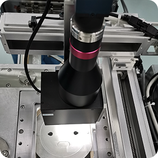
Schottky F.E. emission electron gun
The high brightness Schottky field emission electron source ensures that the high resolution imaging can still be achieved at high magnification.
back


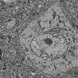
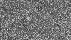
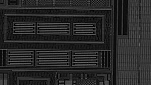
Both owned hardware and software design, the world's fastest dual-channel simultaneous imaging of secondary electrons and backscattered electrons: video-level high-resolution imaging (2×100M pixels/sec).It able to take 600 million pixel super HD image (area: 50μm×50μm, resolution: 24K×24K) in 6 seconds. Compared with the traditional scanning electron microscope, its scanning speed is more than an order of magnitude higher.
High-definition video-level camera frame rate (2×200 frames/sec@512×512, or 2×60 frames/sec@1024×1024). Allow observation of the sample dynamic changes in real time.
| Parameter type | value |
| Resolution | 1.5nm@1kV 1.3nm@3kV |
| Accelerating Voltage | 0.1 kV - 12 kV |
| Magnification Zoom | 500X - 600,000X(SEM) 1X - 500X(Optical) |
| Beam Current | 50pA-300nA |
| Image Size | 512 x 512 - 24k x 24k |
| Image Rate | Dual-channel simultaneous acquisition of 2x100M pixels/sec dwell time is 10 ns/pixel |


 View video
 Product Introduction
 Feature and Benefits
 Technical Specifications
 Related applications and cases