


English
English

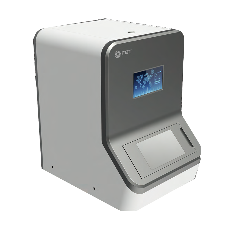
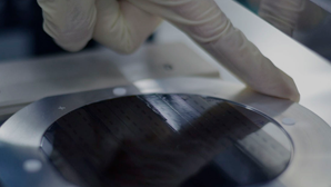
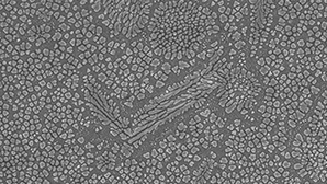
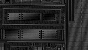
In the field of materials, the ultra-high-speed scanning imaging capability of the high-throughput (field emission) scanning electron microscope. Integrate with the fully automatic focus tracking system and AI image processing algorithm. Enable high-resolution fully automatic detection of samples in a large area (150mm*150mm).
Continuous matrix scanning and automatic stitching to obtain large-scale nano-resolution panoramic map imaging, allows the ability of cross-scale combined information ability and cross-scale material characterization from nanometer to millimeter.
Installation site: No. 76, Xueyuan South Road, Haidian District, Beijing
Application usage: Material engineering (analysis of metal inclusions)
Quantities of assets: 1
Installation period: year 2019
Operation status: Synchronous normal operation


