English
SEM applications
Application field
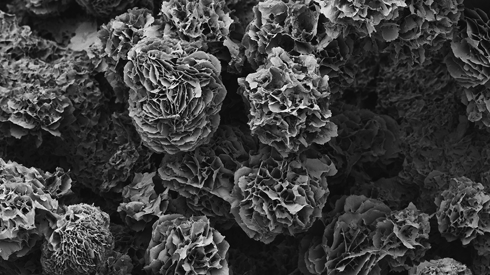
Field emission scanning electron microscope are used to investigate the ultrastructure of a wide range of biological tissues and cells.
→
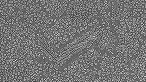
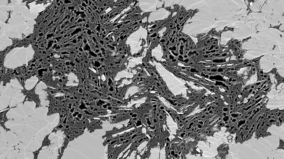
The NavigatorSEM-100 high-throughput scanning electron microscope, with high imaging resolution and long depth of field, can observe and analyze surface morphology of various materials
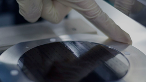
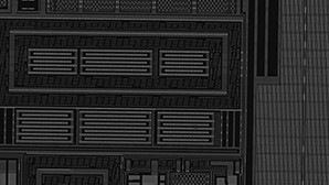
Scanning electron microscopes allows observation of the microstructure and morphology of the surface materials of semiconductor devices
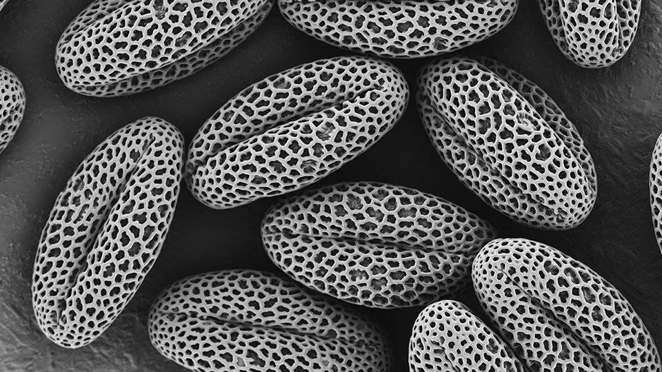
Scanning electron microscope (SEM) imaging is more intuitive and has a certain three-dimensional sense, which can provide extremely useful and rich information for scientific research experts.
20.Material is the material basis for human survival and development.
Sale Enquiry:010-67832505
Technical Support: 4006 507 865
Email:contact@focus-ebeam.com
Address:8101, Building No.8, No.8 Hongda North Road, BDA, Beijing, China 100176
View all contact information
Interest FBT
WeChat Subscription
FBT