


中文
中文

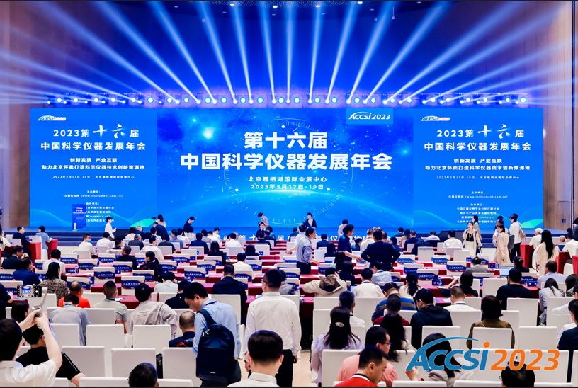
2022年6月21日至6月23日,一年一屆,東南亞最具影響力的半導體展覽會“SEMICON Southeast Asia”,在馬來西亞槟城國際會展中心舉辦,聚束科技(北京)有限公司(以下簡稱“聚束科技”)新加坡分公司(Focus e-Beam Technology Pte. Ltd.)受邀參展。
多年來專注于半導體設備的馬來西亞半導體展覽會 SEMICON Southeast Asia,旨在用最高效的方法收集觀衆對行業的看法,緊跟市場潮流掌握最前沿資訊,為各國半導體市場的從業者提供一個最完善的、面對面的技術交流合作平台,讨論行業的新概念、新趨勢和發展空間,給企業創造最佳契機用以挖掘與開發東南亞市場。
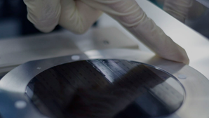
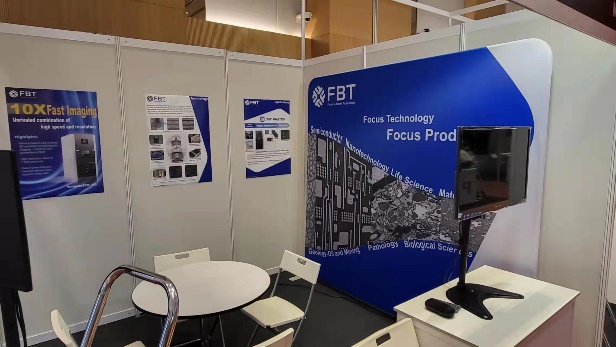
在各大知名儀器廠商雲集、新産品新技術集中亮相的展會現場,展位位于N515的聚束科技,攜高通量場發射掃描電鏡NavigatorSEM-100及其半導體領域解決方案,期待與來自世界各地的專業觀衆進行的深度交流。歡迎各位朋友莅臨參觀!
Focus e-Beam Technology, established in 201Focus e-Beam Technology, established in 2015,consists of multinational innovators and R&D professionals who have decades of experience in electron microscope in the semiconductor industry. We sustain our product development with strong technical knowledge, continuous R&D and partnerships with key industrial players.
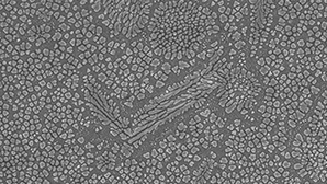
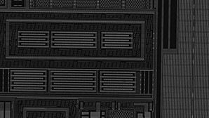
From these synergies, we bring forth to the world our electron microscope: NavigatorSEM-100. It features our propriety Schottky field emission gun, efficient nano-scale imaging and big data analysis AI. NavigatorSEM-100 meets such demand for high throughput and automation in the scientific and industrial communities.
NavigatorSEM-100's patented Direct Electron Detector delivers the best signal to noise ratio for both SE and BSE channels and also collects image data at extreme speed of 100M pixels/sec. Not limited to that, its patented gun-column architecture also offers the largest field of view and highest resolution in the industry.
Therefore, NavigatorSEM-100 excels in industries that require high resolution, high throughput, large area, large volume analysis. Life science, material science, semiconductor.